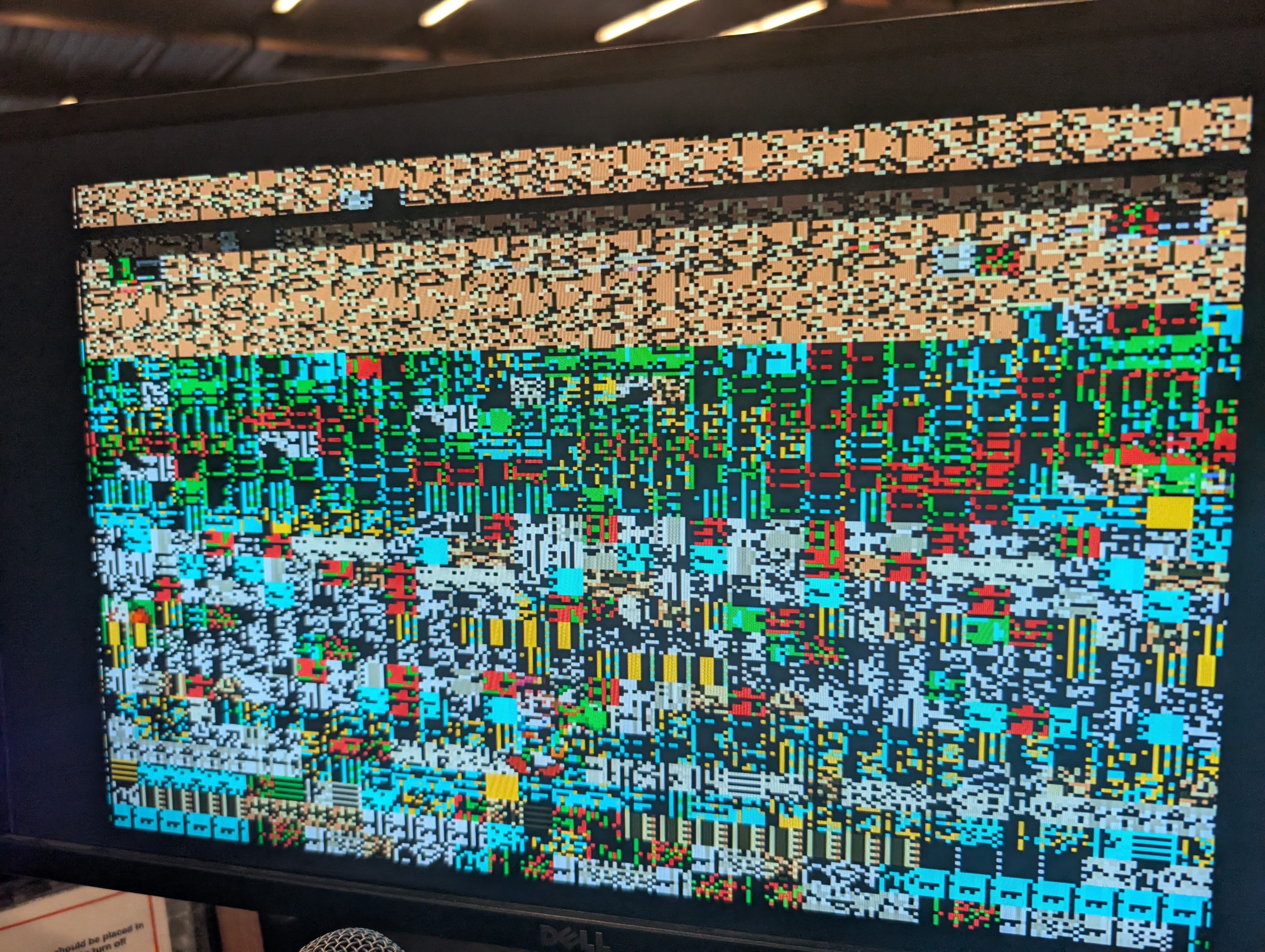
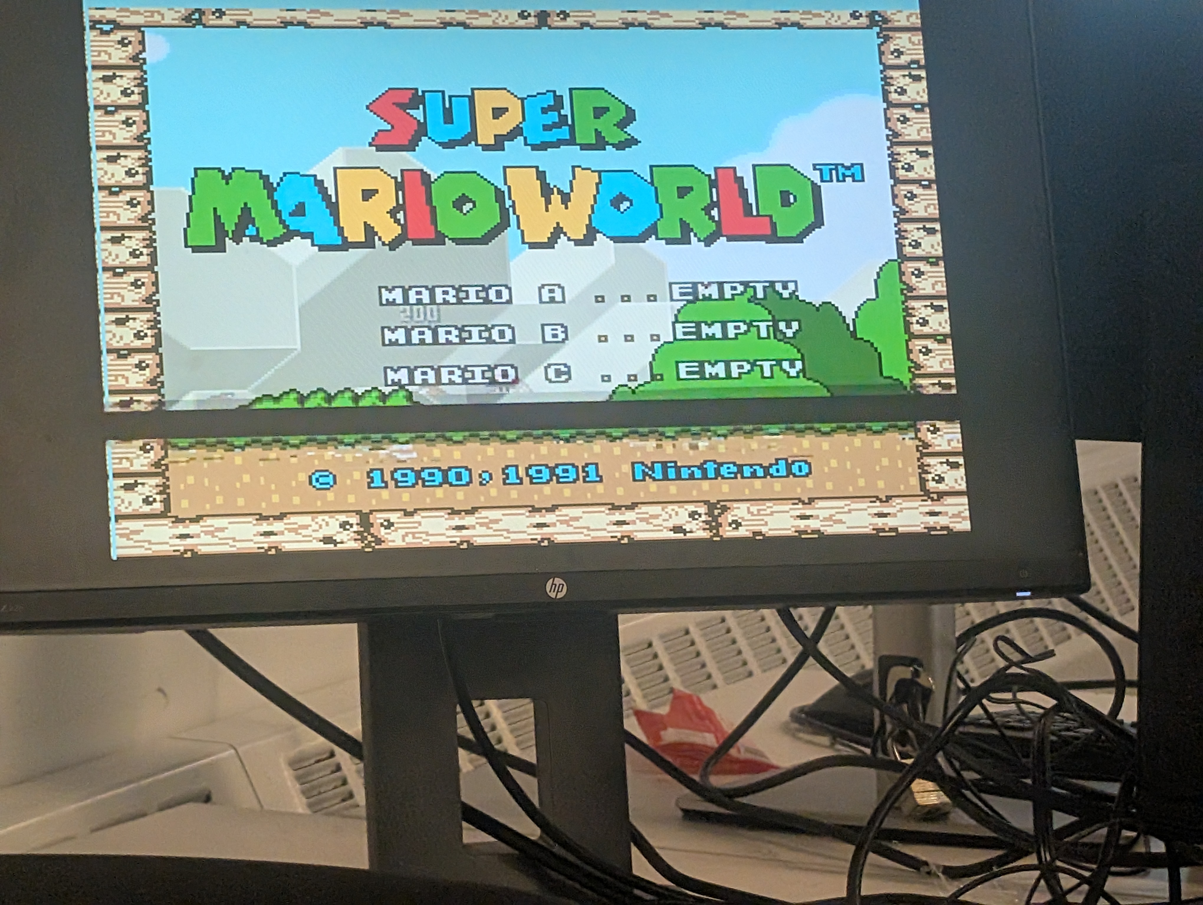
This project began as the final assignment for UIUC's digital design course: build something meaningful with the FPGA. As lifelong Nintendo fans, my partner and I knew early on that we wanted to create some kind of game system.
After learning that no previous team had successfully built a Super Nintendo emulator on the Urbana FPGA board, the direction became clear. We wanted to push our FPGA and computer architecture skills as far as possible and attempt something that had not been completed in the course before.
That simple goal carried us through five intensive weeks of architecture work, debugging, timing analysis, and rendering experiments.
Design
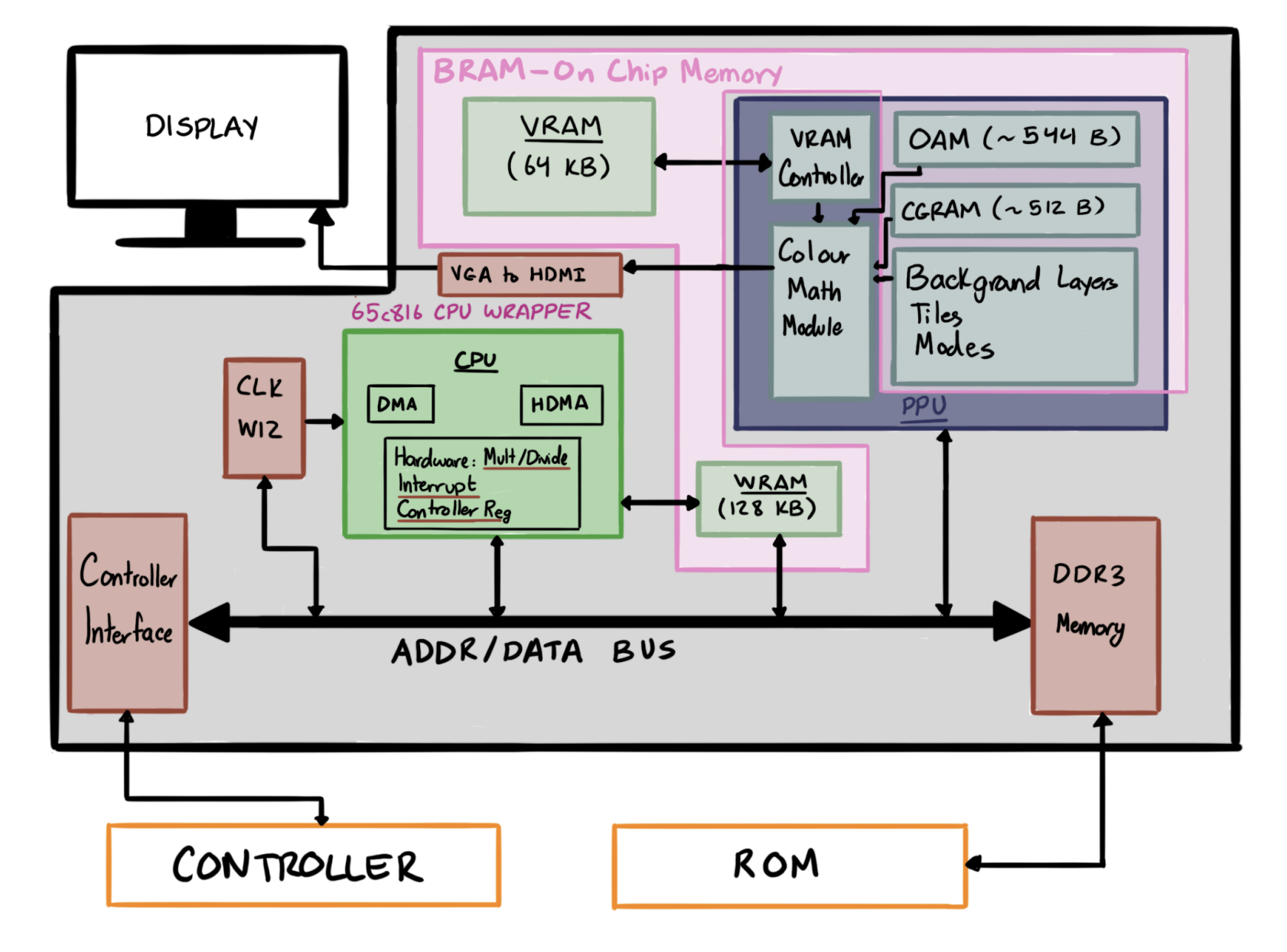
The emulator was built primarily on the Urbana FPGA board, with nearly every subsystem developed from the ground up. The only major components adapted from the open-source SNEStang project were the APU and the 65C816 CPU core.
We designed and integrated the following modules ourselves:
PPU (Picture Processing Unit)
DMA Controller
VRAM Controller
Sprite Renderer
Controller Interface
HDMI Video Output
Memory Arbitration Logic
USB Controller Support
DDR3 Support for ROMs
System architecture showing the CPU, PPU, memory, controller, and display interfaces.
Memory Constraints
Roughly 90% of the system runs directly on the Urbana board. ROMs are stored in DDR3 memory, while BRAM is used for WRAM, VRAM, OAM, CGRAM, rendering buffers, and controller state.
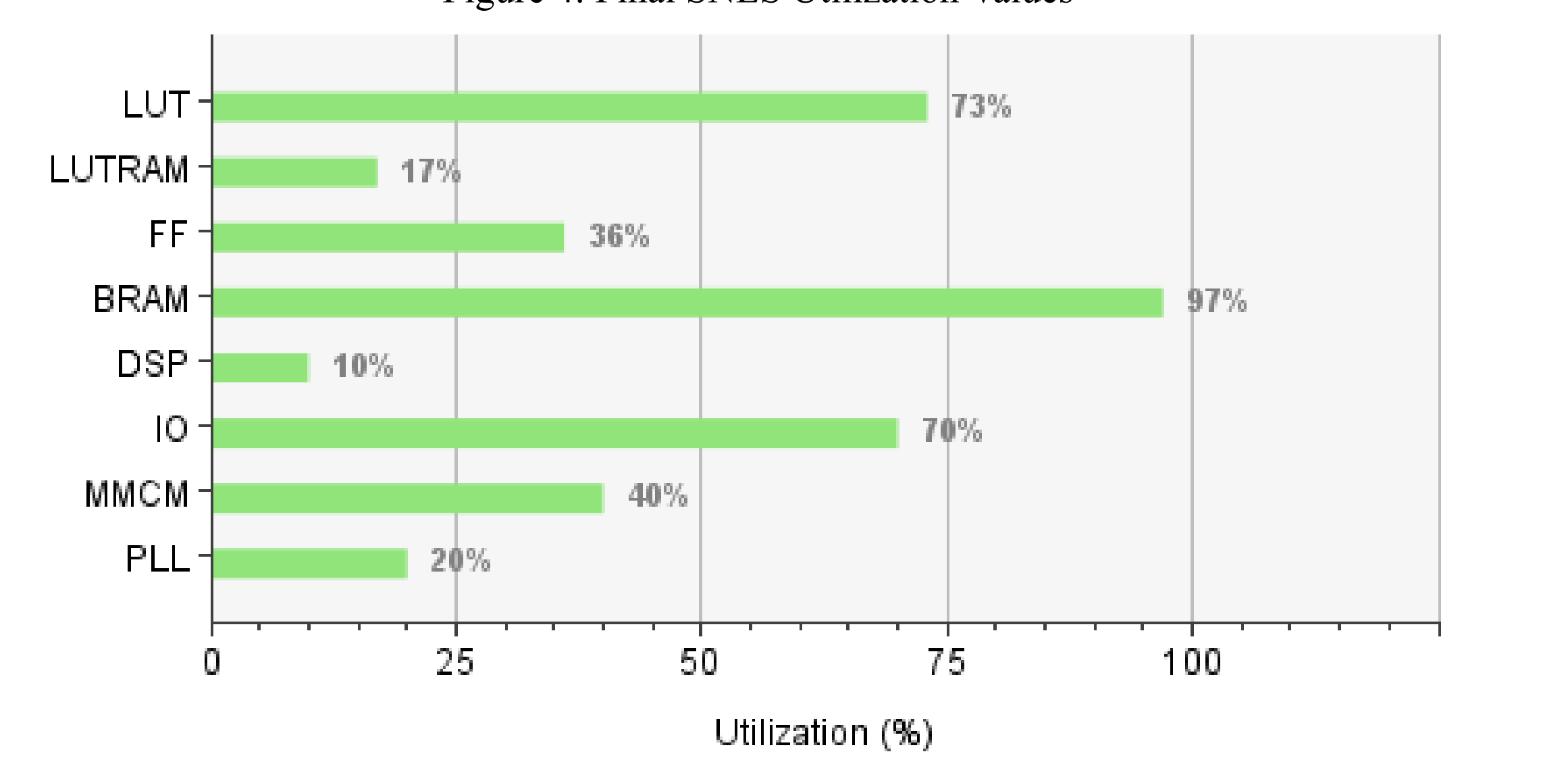
During development, we exceeded the available BRAM after adding the line and frame buffers required by the rendering pipeline. To recover that space, we moved the controller logic onto a Raspberry Pi 4, which communicates with the FPGA through GPIO and jumper wires.
Final FPGA resource utilization, including 97% of available BRAM and 73% of lookup tables.
Rendering Pipeline
The most difficult part of the project was fetching and processing enough graphics data within the available clock cycles. The FPGA's BRAM introduces a one-cycle read latency, while each pixel may depend on as many as four background layers, one object layer, and the color palette.
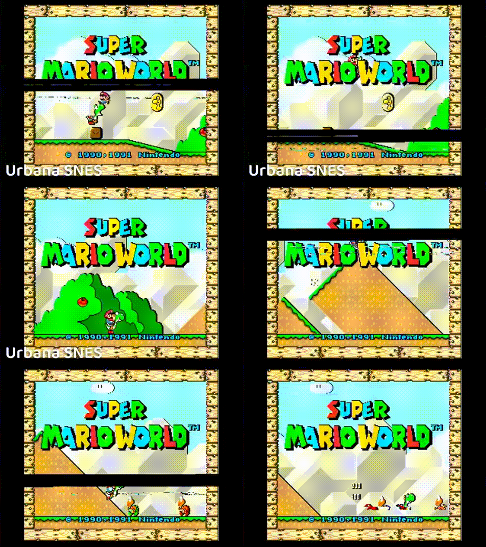
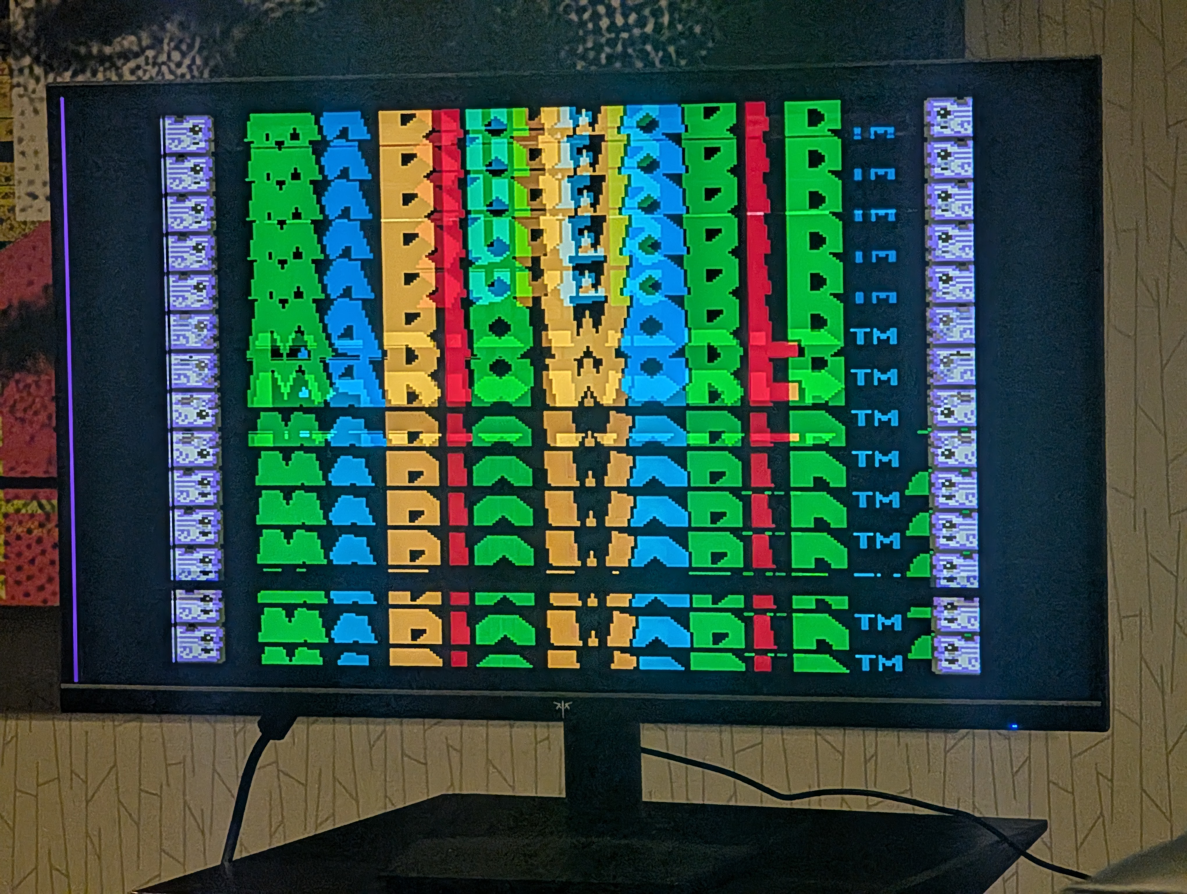
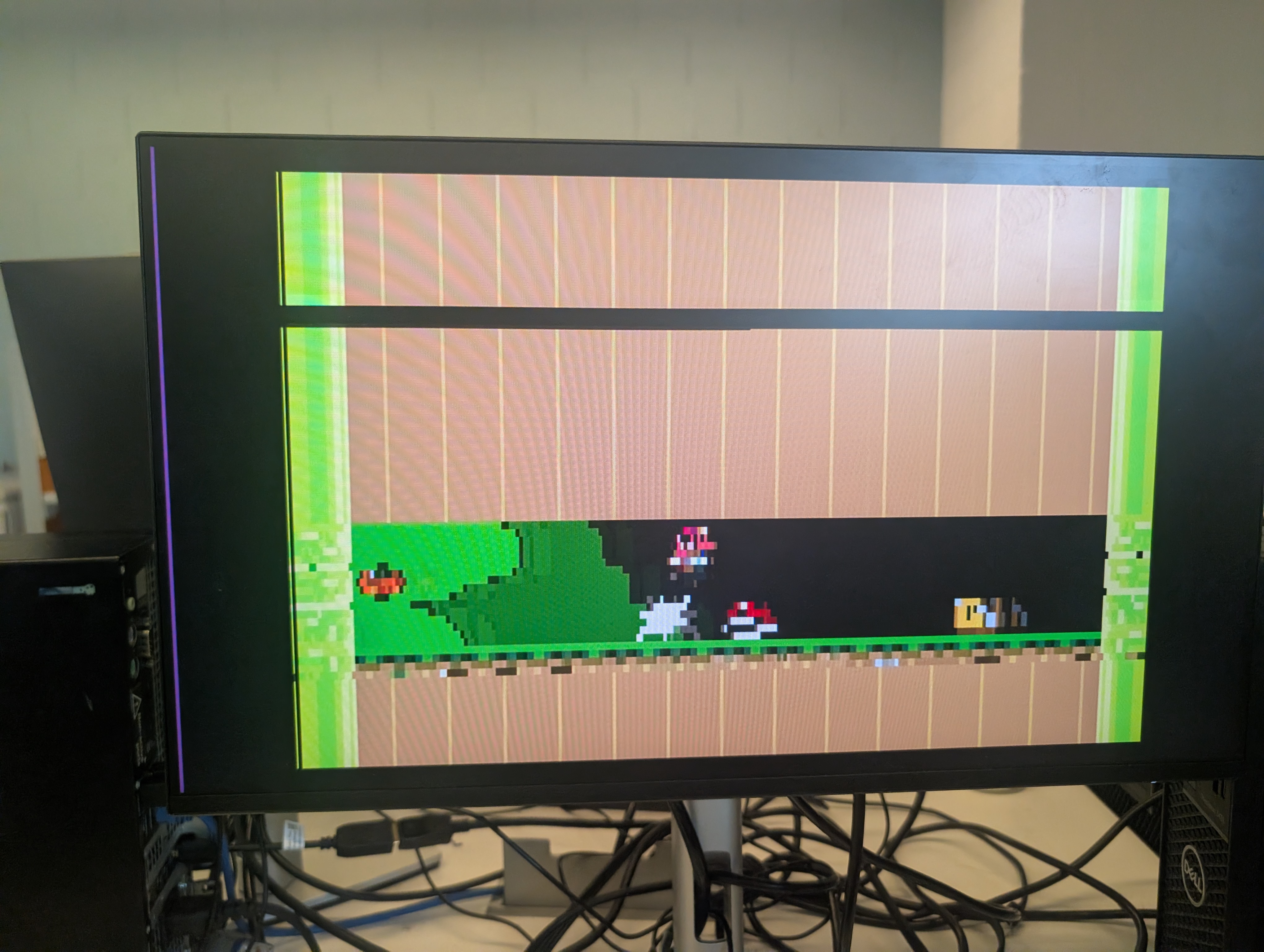
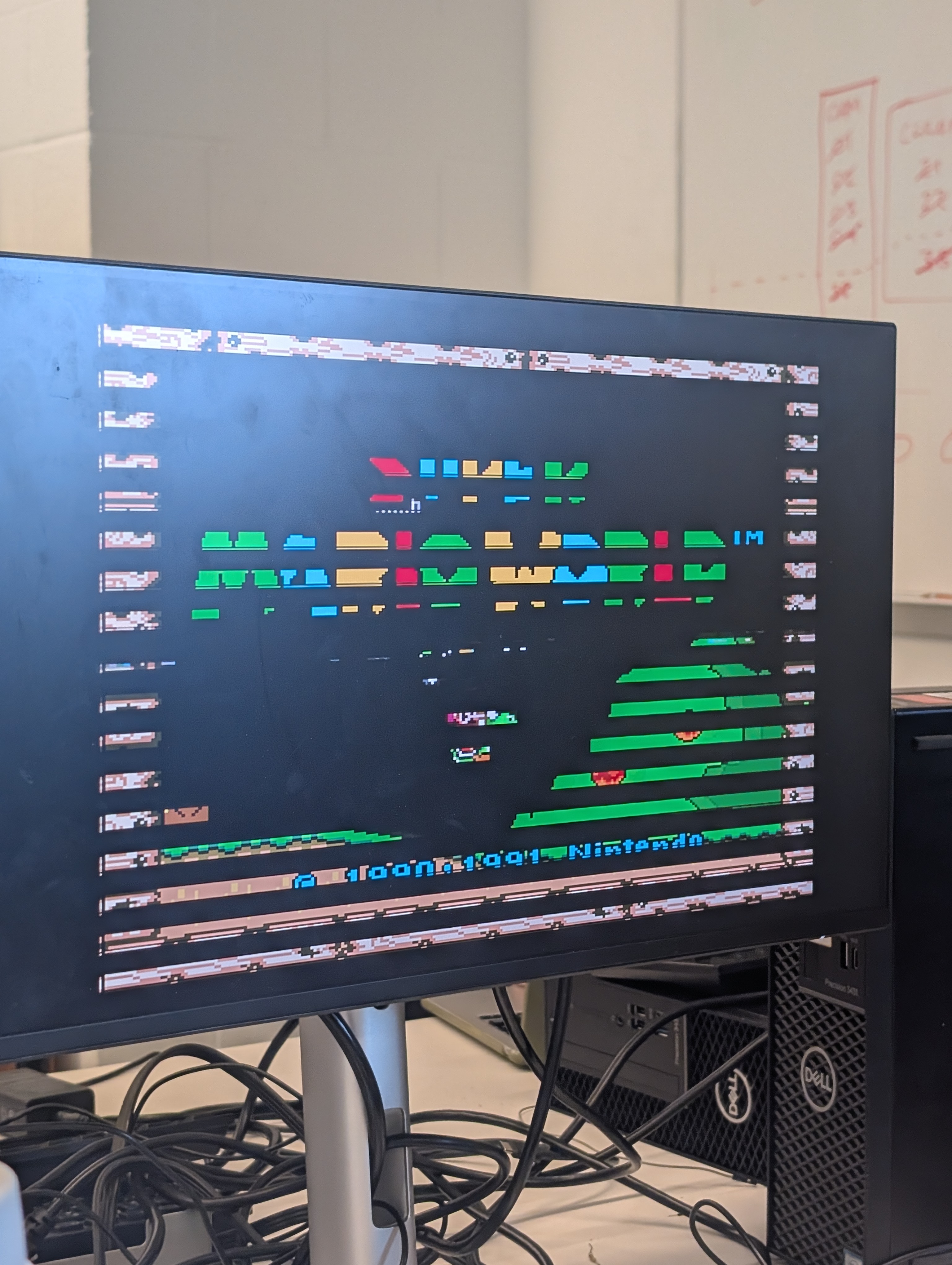
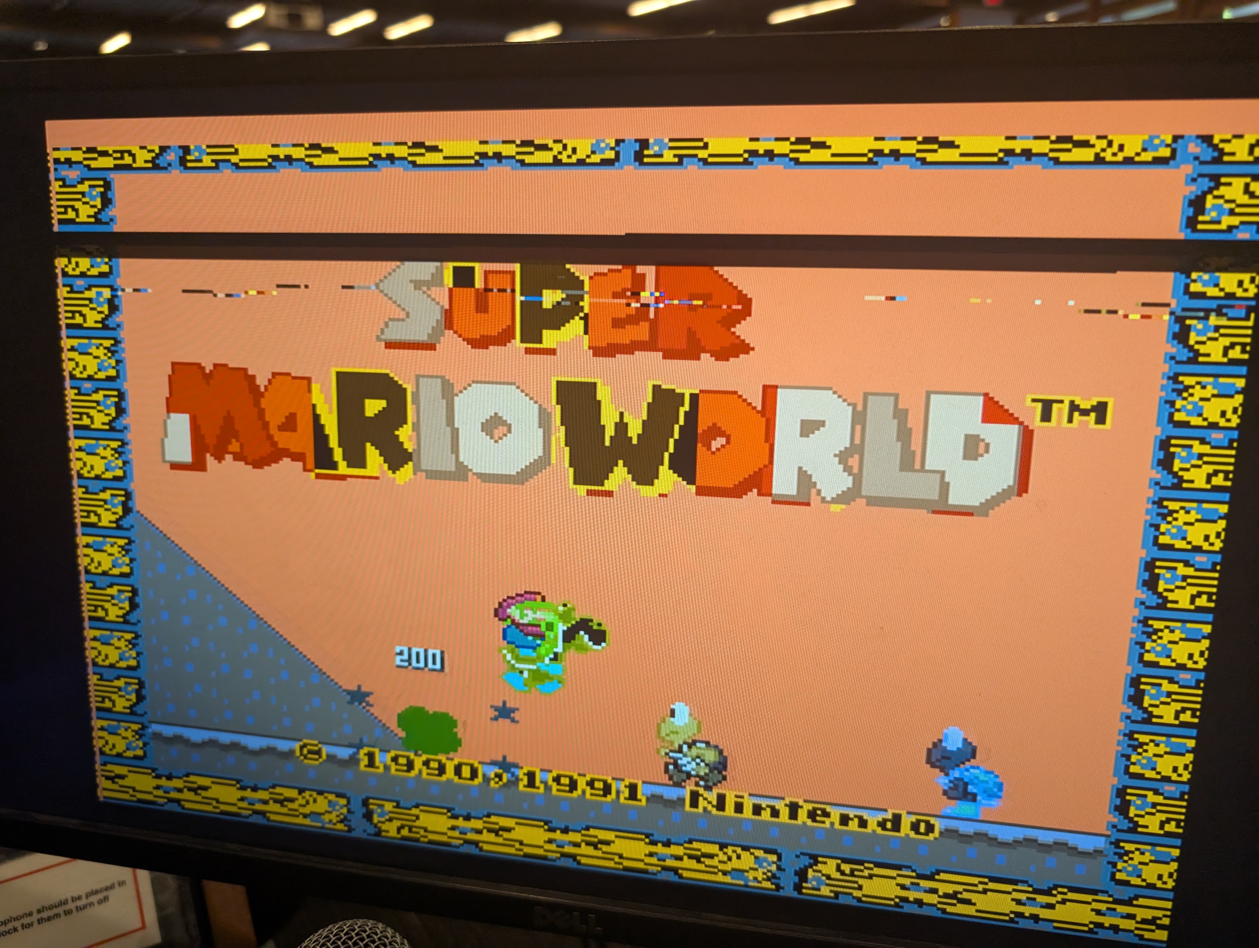
At native SNES timing, our first implementation could not fetch all of that information quickly enough, which produced visible rendering bugs. We explored several solutions, including frame buffering, line buffering, pre-rendering portions of the screen, and splitting the pipeline across multiple processes.
Because we began the project with limited experience in graphics pipelines, a significant portion of the work involved studying and comparing different approaches before converging on an architecture that could reliably produce the expected output.
Scope and Priorities
We chose not to recreate the CPU because the main goal was to understand the rest of the console's architecture and rendering behavior. Our course had already provided substantial experience designing processors and instruction-set state machines, so we focused our limited time on the PPU, memory system, controllers, and video pipeline instead.
The linked report contains the complete architecture, design decisions, and memory breakdown. A high-level system diagram and memory usage summary will be included below.
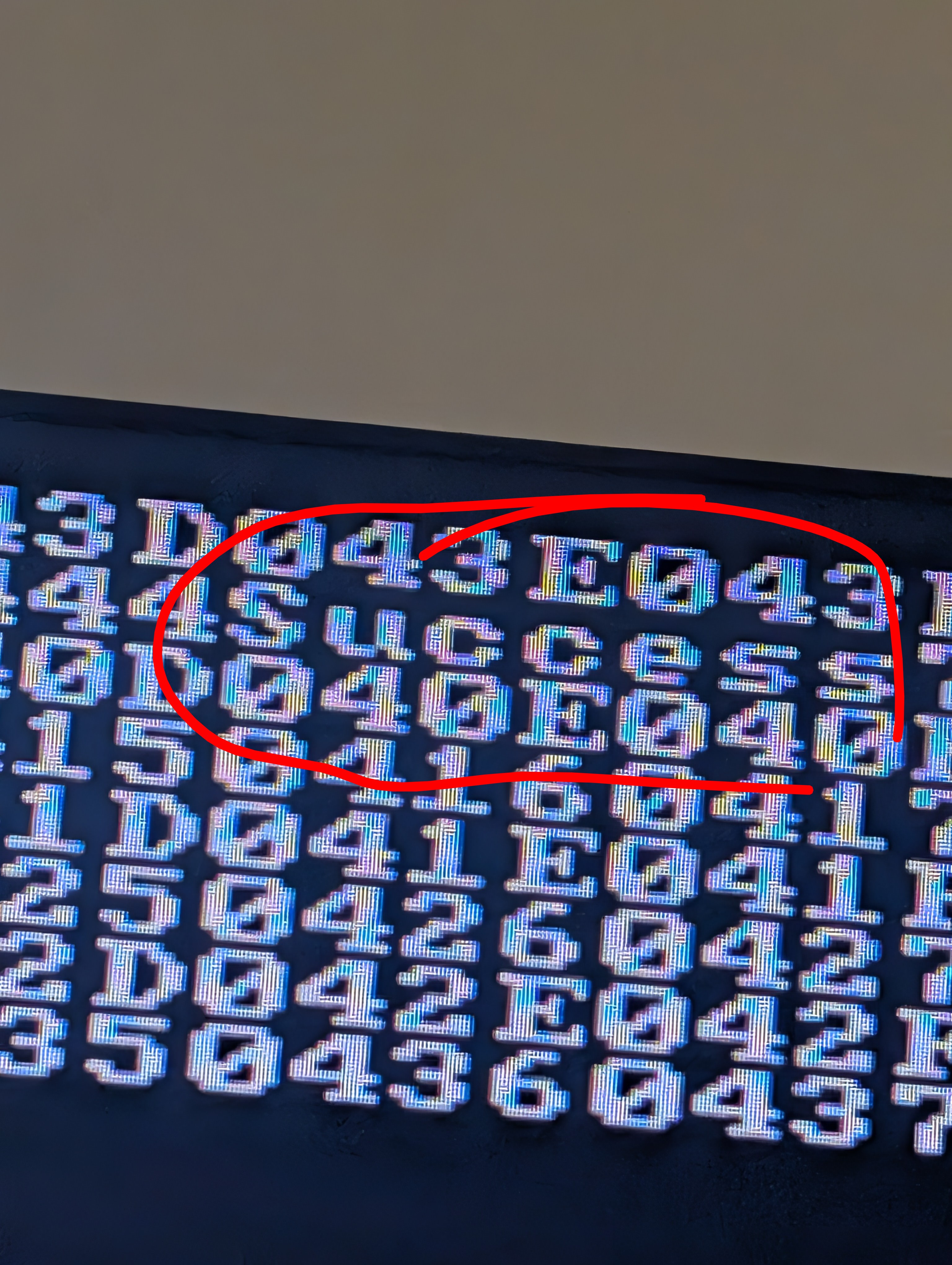
First visible output on the displayGolden CPU test passedSuper Mario World loaded for the first time, background onlyFirst iteration of object rendering
Rendering pipeline debugging
Mario becomes partially legibleFirst complete game load with minor rendering issuesFirst gameplay with rendering issuesHorizontal line artifacts resolved
More rendering bugs
Subscreen rendering workingEarly Super Metroid renderingEarthBound running successfully